This plugin is for use with gEDA PCB. It provides cross-hatching for ground planes. When designing printed circuit boards, there are two areas where such a feature is of interest.
The plugin is compiled with gcc, and works on Linux, OSX, and Windows. See the README for details.
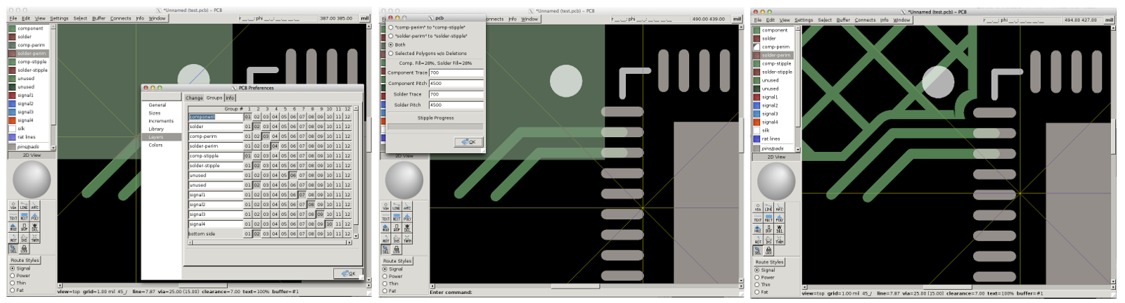
In the first screen above, an example of layer groupings is shown. The "comp-stipple" layer is linked with the "component" layer, while the "comp-perim" layer is independent. A single simple polygon is illustrated on the perimeter layer in this example, but normal use might include any number of overlapping polygons of most any shape. The stipple process calculates insets for pins, pads, and lines, and for a border for the union of any contiguous region. Note that all of these structures are flashed, and no painting of any kind is used. The UCamco technical note "Gerber Format Application Note - Painting Considered Harmful" explains the problem with simply painting lots of lines to achieve the illustrated effect.
The plugin is started using a "sp" command (after typing ":" to get a PCB command line). The resulting dialog box is accepted, and the process executes. When complete, the "comp-stipple" layer is populated as illustrated. Note that the artifacts that PCB shows along its polygon intersections do not in general appear in finished boards. One must examine a finished board under a microscope to confirm this. This is because the plugin uses the Boost library for calculations, rather than the PCB internal polygon routines.
The polygons from a single layer of a pcb are used as a template for stippling a region. First, the intersecting polygons are merged, and a bounding box is drawn around the set of intersected polygons. This set is inserted to a second (presumably empty) layer of the pcb. Then, holes are poked in the polygons, with bounding boxes around all vias, lines, and element pads.
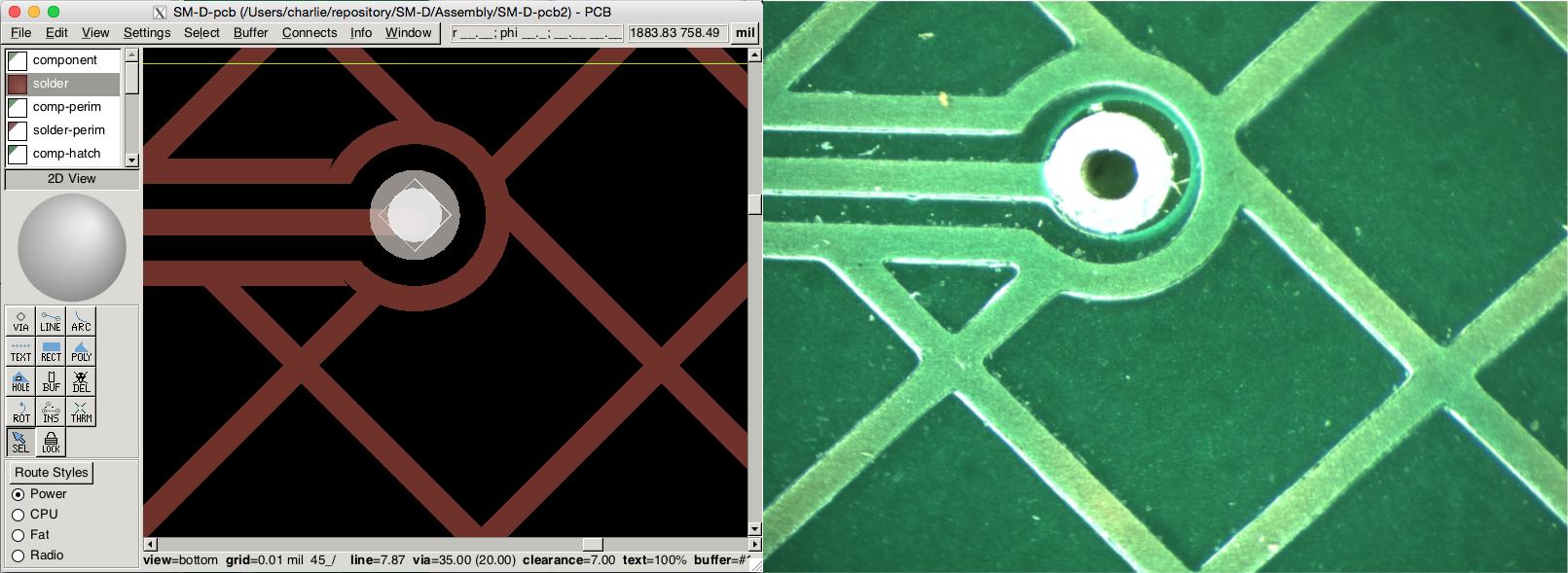
The image at the left shows a slice taken out of the via anuulus in a PCB rendered session. The image on the right, however, is a picture of a board made from Gerber files exported from this design. Note that the flashing does not occur in the finished board as pictured. In general, the polygon artifacts rendered by PCB do not necessarily distort the fabricated board.
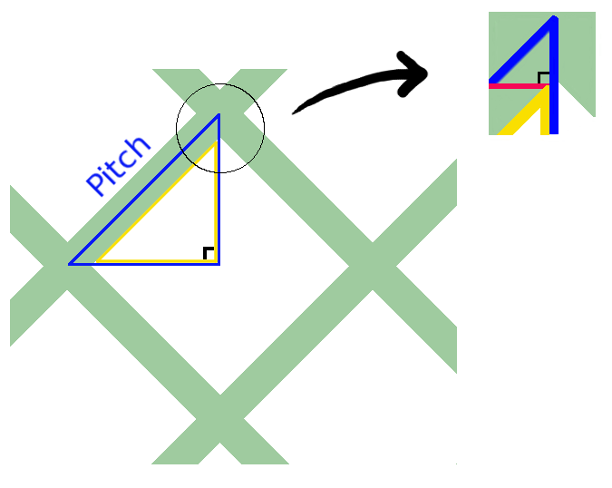
Some sources (e.g. Cypress Semiconductor AN2292) describe a hatch pattern of 7 mil traces with a 70 mil pitch as a ten percent fill. The method for calculating the reported percent fill here is different. Remembering the formula for the area of a isosceles right triangle (and using symetry):

Although one may construct ground loops through a set of adjoining polygons with a large hole in the middle, this plugin will fill them. If this is really what is desired, one might construct a set of disjoint border polygons connected with unstippled polygon slices to form an effective ground loop. Note that in general, ground loops form an antenna of some geometry-dependent resonant frequency, and are typically avoided in PCB design.
This program was written by Charles Repetti, who can be reached on the gEDA mailing list.
 1.8.9.1

